JTAG is unnecessarily confusing, because JTAG is often confused with boundary scan, which is just one of its possible functions.
JTAG is simply a communication interface designed to allow communication to functions contained on devices, for the designed purposes of initialisation, programming, testing, debugging, and anything else you want to use it for (as a chip designer).
Think of JTAG as I2C for testing. It doesn't define what it can do, just a logical interface that allows a uniform channel for communication.
See
The first page (among other things) shows a logical representation describing how multiple devices are wired up using JTAG. JTAG does not specify, data rates or interface levels (3.3V/1.8V, etc) each device can support different data rates/interface logic levels. How to wire them in a compatible way is an exercise for an engineer.
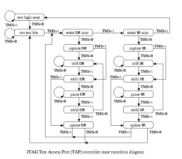
Basically TMS controls which shift register is placed on the device, between TDI and TDO. The second diagram shows the state transitions on TMS which will select different shift registers.
The first thing you need to do is reset the state machine, because when you connect to a chip you do not know what state the controller is in,you need to clock TMS as 1, at least 5 times. This will put you into "Test Logic Reset" State. Knowing this, you can, once reset, then track what each transition on TMS will do, and hence know what state the JTAG state machine is in.
There are 2 "types" of shift registers. The Instruction shift register and the data shift register. The sizes of these are undefined, and can change from chip to chip. The Instruction register is used to select which Data register/data register function is used, and the data register is used to read data from that function or write data to it.
Each of the states control what happens to either the data register or instruction register.
For example, one of the data registers will be known as "bypass" this is (usually) a single bit which has no function and is used to bypass the chip. Assume we have 3 identical chips, wired up like the picture(wikipedia) and each has a 3 bits instruction register, and there are 2 known instructions (110 = bypass, 010 = "some other function") if we want to use "some other function", on the second chip in the line, and not change the other chips we would do the following transitions.
From Test Logic Reset, TMS goes:
0 1 1 0 0
which puts every chip in the chain into the "Shift IR state" Then (while holding TMS as 0) TDI goes:
0 1 1 0 1 0 0 1 1
which puts the following values in the instruction shift register for each chip [110] [010] [110]
The order is reversed, because we shift out the least significant bit first. Then we transition TMS:
1 1 1 0 0
which puts us in the "Shift DR state".
Now when we clock data onto TDI (again while holding TMS to 0) , the data shifts through the data registers, and because of the instruction registers we selected ("some other function" has 8 bits in its data register), our total data register in the chain looks like this:
0 00000000 0
The first and last bit are in the "bypassed" chips, so values read from them are irrelevant and data written to them is ignored. But we need to write bits for those registers, because they are in the chain.
If we wanted to write 0xF5 to the data register we would clock out of TDI (holding TMS to 0):
0 1 0 1 0 1 1 1 1 0
Again, we are clocking the least-significant bit first. Then we would clock TMS:
1 1 0
which updates the selected data register with the value 0xF5 and returns us to run test idle.
If we needed to read the data register before over-writing it with F5, no sweat, that's already done, because the TDI/TDO are set up as a circular shift register, so if you write enough bits to fill the shift register, you will receive the "captured" contents of the data registers simultaneously on TDO.
That's JTAG in a nutshell. On top of this, you need to get specs for target chips and work out what the various instruction registers/data registers do, so you can actually do something useful. That's where it gets interesting. But in and of itself, JTAG is actually very simple.
More Reading
A separate primer contains information about JTAG Boundary Scan Primer for developers that want to extend OpenOCD for such purposes.